Session 7 : Manufacturing
Making electronic components
Before going any further it is necessary to have a basic understanding of what electronic components are and how they are made. Electronic components are generally classified into different families according to their function and physical properties. There are many ways of classifying them but there are three main categories: active components (diodes, transistors, ICs, optoelectronics, displays), passive components (resistors, capacitors, sensors, etc.) and electromechanical components (switches, fuses).
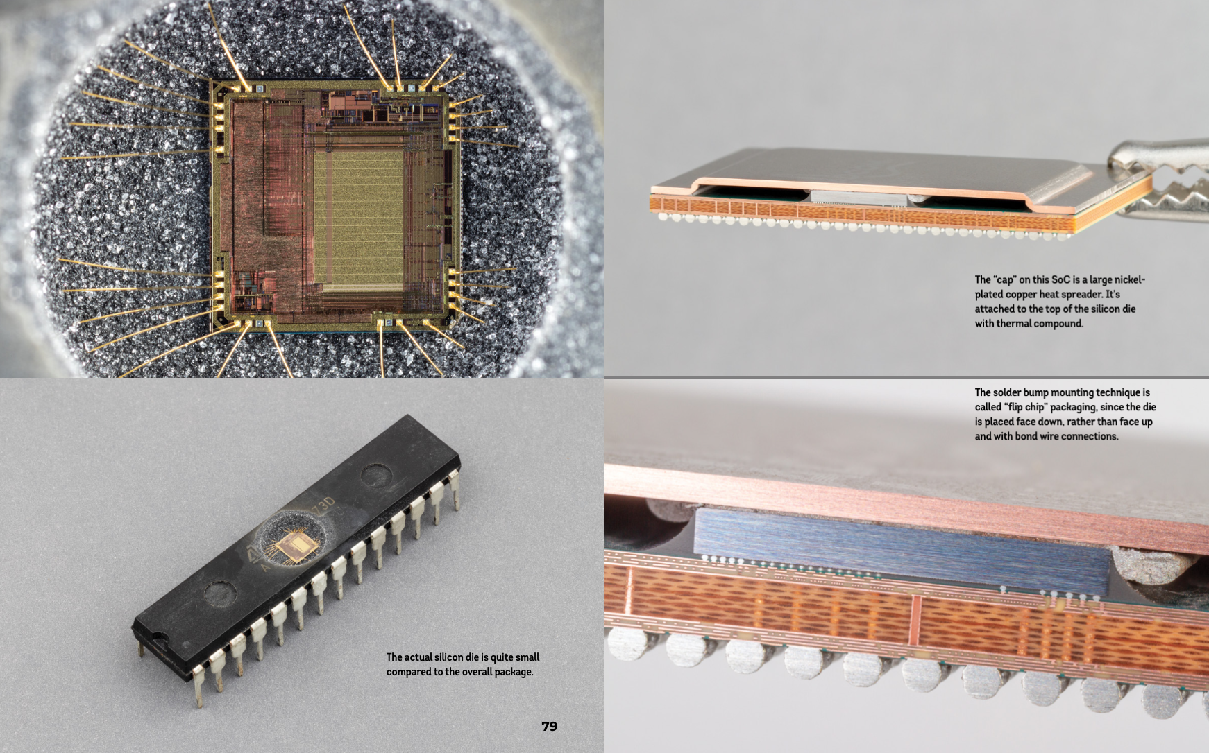
Close-up of a microcontroller (left) and side view of a microprocessor (right) - Credits: Eric Schlaepfer and Windell H. Oskay
Within the integrated circuits there are still different families, called logic, i.e. with logic/electronic gates (diode/transistor/resistor logic). The integrated circuits that interest us are the CMOS (Complementary Metal Oxide Semiconductor) logic components used for microprocessors or memory components.
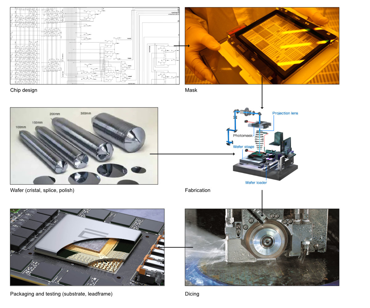
Manufacturing process for ICs
Processors are etched on silica disks, called wafers, doped with another element (e.g. Boron) to modulate their electrical and structural properties. The electronic circuit patterns are affixed to masks that guide the etching, like the negative of a photograph. A wafer allows many circuits to be etched at once, and these circuits are cut with a saw. They are then packaged, i.e. the component connectors are plugged in and tested, and placed in a plastic frame to prevent damage. These components are then sent downstream to the other industries to be soldered onto a circuit board.
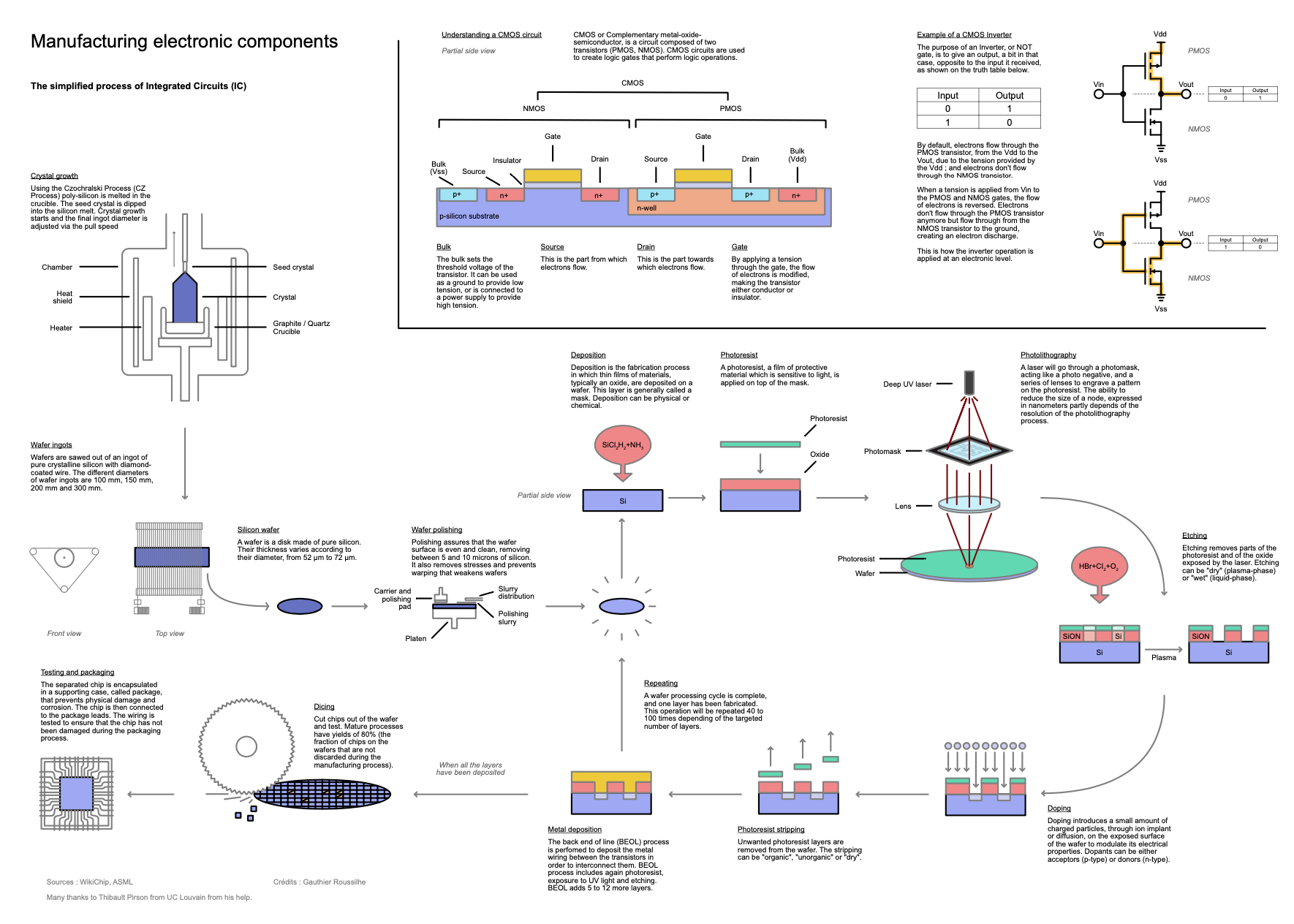
Simplified processes for making ICs, see high-res here
The machines that allow this type of production are very expensive, especially those for engraving. Every year manufacturers produce smaller transistors and can therefore fit more on the same surface. The more transistors there are, the more computing power there is. Today, the most advanced methods engrave at 5nm (the distance separating each transistor from the other) but the physical limit is 2nm and we will reach it within a decade. Today, there is only one type of process that allows us to etch below 7nm, and that is Extreme Ultra Violet. Only one manufacturer produces machines using this process, ASML, and 90% of the production capacity below 10nm is located in Taiwan
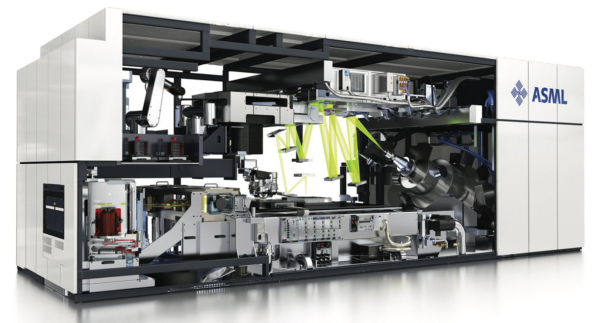
NXE:3400 machine from ASML
Environnemental impacts of engraving
This section uses the research paper from Pirson, Thibault ; Delhaye, Thibault P. ; Pip, Alex ; Le Brun, Grégoire ; Raskin, Jean-Pierre ; et. al. The Environmental Footprint of IC Production: Review, Analysis and Lessons from Historical Trends. In: IEEE Transactions on Semiconductor Manufacturing, Vol. 36, p. 56-67 (2023) http://hdl.handle.net/2078.1/268615 – DOI : 10.1109/tsm.2022.322831
Technological advances have led to a reduction in engraving size. However, this reduction implies an increase in the industry’s use of resources (water, energy, gas, etc.) and the associated environmental impact.

> In conclusion, [...], we show that the environmental impacts per area are clearly increasing with technology downscaling below 0.13 μm. This is observed both in the scientific literature and in LCA databases, despite the scope mismatch. It also seems that this increase is accelerating for advanced nodes

_Node-wise trends based on data from the scientific literature and the LCA databases. This shows the environmental impacts per cm2 with respect to (b) GWP, and (c) water consumption_
In addition to the relative impacts increase in engraving per unit area, the size of chips tends to increase in order to accommodate an even greater number of transistors.
 _Transistors count and die size per release date for CPU (blue) and GPU (orange), [chip-dataset](https://chip-dataset.vercel.app/) _
Thus, although the environmental impact per transistor, or more generally per unit of computing power, is decreasing, the environmental impact of chips is also increasing significantly, as is the number of chips produced, which is leading to an increase in the global impact of the semiconductor industry. This is a classic example of the rebound effect.
Wafer Losses
In progress…